

Why Cell Balancing Safety Matters
In any multi-cell lithium pack, the sensing and balancing lines are everywhere. A large electric vehicle (EV) battery energy storage system (BESS) may route dozens of fine conductors between each cell, the battery management system (BMS), and the analog front end (AFE). That is a lot of potential fault paths, and they do not all fail the same way. Shorts can occur between random lines from assembly mistakes, mechanical accidents, or contamination that creates conductive deposits over time.
The scale amplifies the risk. Because there are so many lines, a single failure can cut pack throughput, force costly rework, or create unsafe service conditions. That is why line-level protection is treated as a system requirement in credible BMS design guidance.
Passive vs. Active Balancing
Balancing keeps cell state of charge aligned so the pack is not limited by its weakest cell. In passive balancing, the BMS shunts roughly 50 ~ 250 mA through resistors to trim high-SOC cells toward the average. Active balancing instead moves charge between cells using capacitors, inductors, or DC-DC elements switched through a matrix. It can improve energy efficiency, but it also brings greater cost, complexity, and size.
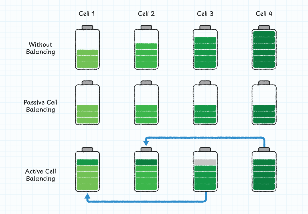
Regardless of the method, the sheer number of sense and balance conductors in EV and BESS modules makes fault protection a critical design priority. Line-level safeguards are essential to maintain system integrity, prevent service disruptions, and uphold safety standards across both passive and active topologies.
The Problem with Fusible PCB Traces
Using copper traces as makeshift fuses may look attractive on paper, but in practice it is an unsafe and unreliable way to protect balancing and sense lines. The “opening” behavior depends on too many uncontrolled variables including:
- Copper thickness and width – “Trace” fuses are highly sensitive to manufacturing variations in trace width and thickness, which directly impacts their current carrying capacity and fusing point. A trace “fuses” by self-heating (I²R) until the copper necks and opens. In practice, copper weight, plating, etch tolerances, and nearby heat sinks all change resistance and cooling, causing the blow current and time to drift widely. Even ‘identical’ traces on one board can reach very different temperatures, altering when and how they open, especially during long, modest overloads.
- Laminate resin content – Resin/glass ratio is not uniform across a panel or even across a weave. That matters because resin controls thermal conductivity, glass transition (Tg), and tracking behavior. Resin rich areas run hotter and char sooner; glass rich areas wick heat away. When a trace finally fails, a resin that chars easily can leave carbonized, partially conductive paths (low CTI), so instead of a clean open you get a high resistance “smoldering” fault that continues to leak current and reignite under stress.
- Epoxy aging – Over time, thermal cycling, humidity, and voltage stress oxidize and embrittle epoxy. Tg drops, microcracks form, and moisture absorption rises, reducing dielectric strength and CTI. An “okay” trace on day one can become easier to carbonize later in life, so the same overload that once cleared marginally now produces charring, conductive residues, or arc tracking. That pushes real-world clearing behavior further away from whatever you measured on a fresh coupon.
- Dendrite growth – Under DC bias, humidity, and ionic contamination, copper can undergo electrochemical migration: metal ions dissolve near the anode and plate out as tree-like filaments toward the cathode. These dendrites can bridge gaps created by a blown trace or create low kΩ leakage paths between sense/balance lines. The result is the worst of both worlds: the “fuse” opened, but a parasitic conductor silently reestablished current, sustaining heating and intermittent faults that are hard to diagnose.
- Repair challenges – “Trace” fuses are not easily replaceable and require PCB replacement or trace repair.
All these items shift the blow current and blow time over life. When these traces finally do fail, they rarely produce a clean, contained open. Instead, they can char or carbonize the printed circuit board (PCB), depositing conductive debris and leaving a partially conductive path that ignites under stress.
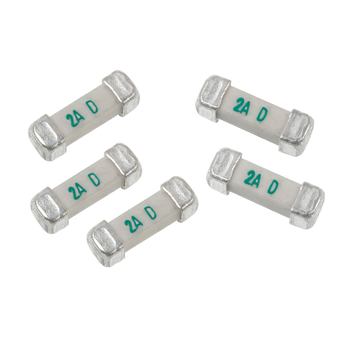
The safer alternative is to use fast-acting SMD fuses, so each line fails cleanly and predictably when a fault occurs, and the event is contained rather than propagated.
Why SMD Fuses Beat Fusible Traces
Purpose-built SMD fuses provide a specified, predictable opening window. Their time-current curve characteristics and I²t behavior are defined, and as a result, they clear faults reliably across a wide spectrum, from milliamp-level abnormalities to high-energy shorts where available current can reach the kiloamp range.
Critically, arcing is contained inside the fuse package, rather than occurring openly on the board. When an SMD fuse operates, it leaves a clean, fail-safe open. That means no charred PCB, no conductive carbon tracks, and no debris spread across the PCB. This sharply reduces the risk of latent, intermittent faults after a “cleared” event.
Unlike improvised trace “fuses,” SMD fuses also allow cascaded protection—for example, a fuse on the flex tail and another on the AFE/module PCB—so you can coordinate which device opens first and localize the fault for easier service. Finally, SMD fuses are available in various sizes and current ratings, RoHS compliant, Halogen-free, offered with automotive qualifications (AEC-Q200) and safety agency approvals, aligning with design practices for EVs and BESS where documented performance and compliance matter; copper traces offer no such qualification path.
| Feature | Fusible PCB Trace | SMD Fuse |
|---|---|---|
| Opening Behavior | Unpredictable; varies with materials/age | Defined time–current curve and I²t |
| Failure Mode | May char PCB, leave conductive residue | Clean open; no debris or carbonization |
| Replaceability | Difficult; requires board repair | Easy; standard footprint, field replaceable |
| Coordination Across Devices | Not possible | Supports cascaded protection schemes |
| Compliance & Qualification | None | RoHS, AEC-Q, UL, etc. |
| Arcing Containment | Occurs on board | Contained within fuse package |
Table 1: Comparison of SMD Fuses vs. Fusible PCB Traces
Table 1: Comparison of SMD Fuses vs. Fusible PCB Traces
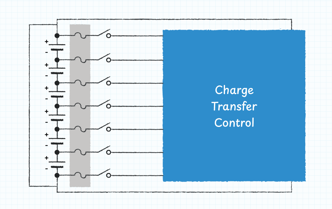
SMD Fuse Placement and Selection for Balancing Networks
Establish a build-ready rule set: specify a surface-mount device (SMD) fuse in every sense or balance conductor, verify its time–current curve and I²t against normal bleed and worst-case cross-cell faults, and define a cascaded opening sequence that localizes faults and simplifies service.
- Placement – Install a series SMD fuse in each sense or balance lead—either on the flex tail or at the analog front end (AFE) header—so the fuse encounters the fault first and opens before heat spreads.
- Sizing – Rate the fuse above the continuous bleed current, accounting for temperature rise and duty cycle, yet low enough to open in < ~1 s under a short.
- Validation – Compare manufacturer time–current curves and I²t data with both steady-state bleed conditions and worst-case faults, then confirm opening times across temperature and tolerance through bench testing.
- Coordination and Cascading – Create a cascaded scheme (flex + printed-circuit board), assign a deliberate opening order, and coordinate I²t with upstream protection so the most local, least disruptive device clears first, and nuisance trips are avoided.
- Surge and ESD Protection – Add transient voltage suppressor (TVS) diodes at AFE inputs and VBAT nodes; select standoff and clamp voltages that respect AFE absolute-maximum ratings, and the transient profile produced by hot-plug events or inductive coupling.
- Thermal Safeguards – Deploy distributed temperature sensors along the stack to detect hot spots early and shut the system down before faults propagate.
- Serviceability and Standardization – For large packs, choose common footprints (for example, 0603 or 1206), label each fuse clearly, and publish a step-by-step replacement procedure to expedite field service and reduce errors.
Safer Balancing Starts with SMD Fuses
Cell balancing keeps packs healthy, but it also exposes a dense web of sense and balancing leads to real world failure modes. “Fusible” copper traces simply do not provide a predictable or contained response to those faults; their blow behavior drifts with materials and age, and their failure can carbonize the board.
In contrast, purpose-built SMD fuses deliver a known time–current profile and I²t, open cleanly, and allow coordinated, cascaded protection so faults are localized and serviceable. The design playbook is straightforward: place a series SMD fuse in every balancing and sense line, size it to pass normal bleed currents without nuisance opening and ensure it clears quickly under cross-cell faults.
The result is a BMS that fails safely, is easier to diagnose in the field, and aligns with automotive-grade expectations for documentation and compliance. In other words, if cell balancing is the “routine,” line-level protection is your emergency plan, and SMD fuses make that plan reliable.
For best results, specify Bel chip fuses on every balancing and sense lead. Contact a Bel expert today to learn more about I²t coordination, part selection, and placement guidelines for safe and effective BESS designs.

.png)