The Power Density Challenge in Modern System Design
Modern power systems, spanning electric vehicles, robotics and automation lines, high-efficiency servers, and solar power inverters, face a shared challenge: delivering more power in smaller, thermally constrained spaces. As system architects push toward higher power densities, they must also contend with switching losses, thermal bottlenecks, and the limitations of traditional magnetic components. This article explores the engineering principles behind compact inductor design and how innovations in flat coil architecture can enhance performance, efficiency, and reliability in high-current environments.
Maximizing Efficiency and Density with Flat Wire Inductors
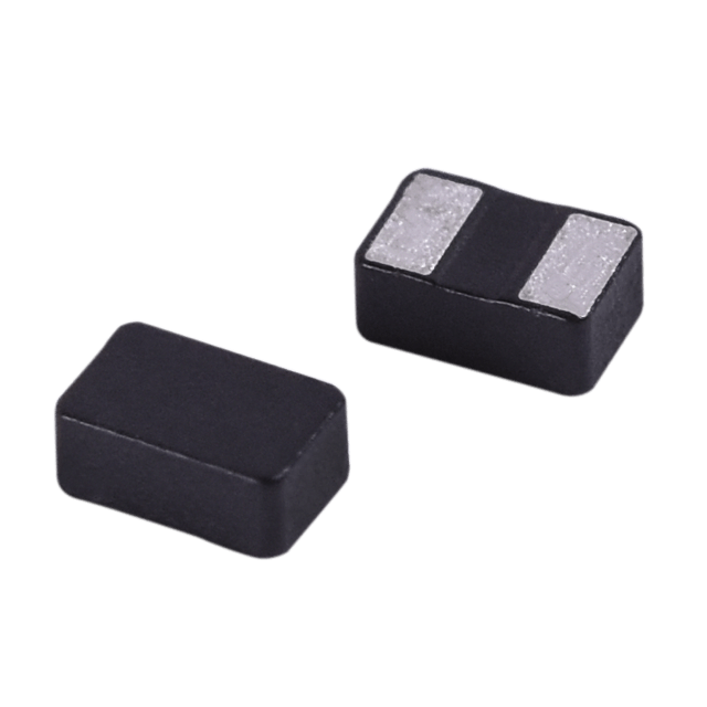
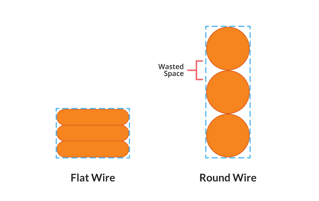
Flat wire inductor technology has emerged as a key enabler for achieving high power density in constrained designs. Unlike traditional round-wire inductors, flat wire coils offer improved thermal performance and reduced AC losses. This makes flat wire inductors ideal for use in DC-DC converters powering GPUs or CPUs (e.g., VRMs), EV power steering circuits, and server boards where tight spacing and thermal control are critical.
One of the primary design advantages lies in how tightly and uniformly the turns can be wound. This maximizes the effective cross-sectional area of the conductor, significantly reducing copper losses and enabling higher current handling without compromising thermal stability. Additionally, flat coil geometries reduce skin and proximity effects, phenomena that increase resistance at higher frequencies, resulting in better efficiency and less heat generation.
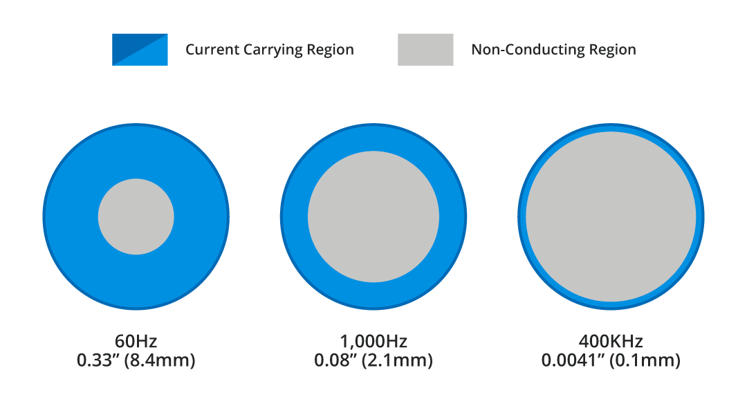
When alternating current (AC) flows through a conductor at high frequencies, it tends to concentrate near the outer surface of the wire. This phenomenon, known as the skin effect, reduces the effective cross-sectional area available for current flow, which in turn increases the conductor’s resistance and power loss.
Understanding Skin Effect in High-Frequency Power Design
The depth to which current penetrates is called the skin depth, and it decreases as frequency increases. In conventional round-wire inductors, this effect becomes increasingly problematic at higher switching frequencies common in modern power electronics. More resistance means more heat, less efficiency, and ultimately larger, less reliable components. In high-speed battery chargers or solar inverters switching in the 100 ~ 500 kHz range, these effects can significantly reduce system efficiency if not mitigated with optimized conductor geometry.
Flat wire inductors help mitigate this issue. Their broad, shallow geometry provides more surface area for current distribution, reducing the impact of skin effect and maintaining low resistance across a wider frequency range. This translates into better thermal performance and higher overall efficiency, particularly in tightly packed, high-power applications.
How to Calculate Skin Depth
Skin depth (δ) defines how deeply AC current penetrates into a conductor before its intensity diminishes significantly. It is influenced by the material’s conductivity, the magnetic permeability, and the signal frequency. The formula for skin depth in a non-magnetic conductor (like copper) is:
Where:
δ = skin depth (in meters)
ρ = resistivity of the conductor (ohm-meters)
ω = angular frequency = 2πf where f is frequency in hertz
μ = permeability of the conductor (typically μ₀ = 4π×10⁻⁷ H/m for non-magnetic materials)
So, at 500 kHz, current only penetrates about 0.093 mm into a copper conductor. Any conductor significantly thicker than this will have portions that carry minimal current, wasting material and increasing losses.
Flat wire designs help align the conductor’s shape with the expected skin depth, ensuring optimal use of material and minimal AC resistance. This is especially valuable in applications operating in the 100 kHz ~ 1 MHz range and beyond.
Proximity Effect and Its Role in Inductor Efficiency
While skin effect limits how deep AC current penetrates a single conductor, proximity effect refers to how nearby current-carrying conductors influence current distribution within each other. When conductors are placed close together, like in tightly wound inductors, AC magnetic fields from adjacent turns can push current toward specific areas of the wire surface. This non-uniform distribution increases the effective resistance and results in additional power loss.
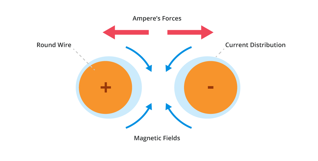
Proximity losses are particularly significant in high-frequency inductors, where multiple turns lie close together and magnetic coupling is strong. These losses scale with frequency, conductor spacing, and winding configuration.
Quantifying Proximity Effect Losses
Proximity effect losses are more complex to calculate than skin depth because they depend on the geometry of the winding and the magnetic fields generated by neighboring conductors. However, in simplified form, proximity loss (Pprox) can be approximated using Dowell’s method for multilayer windings, which is commonly applied in transformer and inductor design:
Where:
k = constant based on conductor and winding geometry
f = frequency (Hz)
Bac = AC magnetic flux density
N = number of turns
d = conductor diameter or spacing between conductors
What Dowell’s Method Tells Us
- Proximity losses scale with the square of frequency and flux density, making them critical in high-frequency designs.
- Losses also increase with the number of turns and inter-turn distance.
- For precision modeling, engineers often use finite element analysis (FEA) tools or empirical testing due to the geometric complexity of real-world inductors. Still, this equation highlights the key design variables engineers can control.
How Flat Wire Reduces Proximity Effect
- Reducing inter-turn spacing: Tighter, more uniform winding helps control magnetic field coupling.
- Maximizing surface alignment: Flat surfaces distribute magnetic influence more evenly, minimizing current crowding.
- Lowering winding height: Shorter vertical profiles reduce field interaction between adjacent layers.
Why Flat Wire Matters in High-Frequency Power Design
In high-frequency, high-current applications, managing AC losses is a fundamental design challenge. Skin effect limits how deeply current can penetrate a conductor, increasing resistance and heat. Proximity effect compounds this issue by forcing current into narrow regions due to magnetic fields from nearby turns. Together, these phenomena can significantly degrade inductor efficiency, thermal stability, and overall system performance.
Flat wire inductor designs provide a robust solution. By offering a broader surface area and tighter, more uniform winding geometries, flat conductors minimize the resistive losses associated with both skin and proximity effects. This leads to better thermal behavior, lower power dissipation, and more compact inductor footprints, without sacrificing performance.
Whether it is minimizing losses in industrial motor controllers or ensuring thermal reliability in dense EV control boards, flat wire inductors enable compact, high-output system design. These characteristics are especially valuable as engineers strive to reduce the size and weight of power systems while increasing output, an increasingly common demand in electric vehicles, server architectures, and renewable energy platforms.
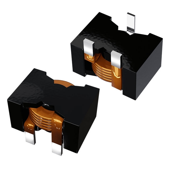
Helical Flat-Wire Winding for Enhanced Thermal Performance
In high-current inductor designs, winding geometry significantly influences both electrical and thermal behavior. When flat conductors are wound in a helical configuration, rather than stacked in a traditional multilayer or orthogonal layout, they offer improved surface contact between adjacent turns and reduce inter-turn air gaps. This facilitates more efficient heat conduction through the winding structure and toward the magnetic core interface or external thermal pathways.
The broad surface area of flat wire inherently supports better heat dissipation, and when arranged helically, it forms continuous thermal channels that promote uniform heat spreading across the winding body. This mitigates localized hot spots and enables more stable thermal performance under sustained high-current operation. Additionally, the enhanced conductor packing and heat transfer allow for increased current-carrying capacity without increasing the inductor's physical footprint, an essential advantage in compact, high-density power applications.
Applying Flat Wire Innovation in Real-World Designs
The engineering principles behind flat wire inductors—reducing skin and proximity effects, improving thermal management, and enabling compact layouts—are not theoretical advantages. They are essential tools in addressing the challenges of modern power electronics. As system designers push the limits of efficiency and power density, component-level innovations become mission-critical.
By aligning fundamental electromagnetic design with practical manufacturing needs, flat wire inductors represent a key enabler for the next generation of compact, high-efficiency power systems.
Looking to reduce AC losses and shrink your design footprint? Explore Bel’s compact flat wire inductors and find the right solution for your application.