In recent years DC to DC switching converters have become popular due to their higher energy efficiency, lower power dissipation and smaller size compared to linear regulators. These advantages match well to the needs of battery powered IoT devices.
The Expanding Role of DC to DC Switching Converters
In response to interest in switching converters, silicon IC manufacturers have widened their portfolio of ICs to support different conversion topologies, input to output voltage requirements and output current capabilities. With the software design tools which accompany these ICs most designs can be rapidly turned into a schematic with simulation plots, PCB layout and Bill of Materials (BoM) - including the required inductor - by almost any designer, whether they previously considered themselves a power supply expert or not.
The Advantages of Switching Converters Over Linear Regulators
With linear voltage regulators it is only possible to step down the input to a lower output voltage. The voltage difference between the input and the regulated output is continuously dropped across the regulator's pass transistor, multiplying with the load current this becomes wasted power consumption, dissipated as heat, with the consequent negative impact on efficiency, battery life and operating temperature. The ability to only step down is limiting if the product design requires a higher or inverted output voltage from the input supply voltage.
Linear regulators are still popular for point of load (POL) applications with low output currents or a small input to output voltage drop, which limits the power lost. In designs where there is a large input to output voltage drop or high load currents, switching converters have become preferred due to their higher efficiency. This is still achieved using a power transistor but now continuously switching the input ON and OFF with the switch duty cycle controlled, such that the resultant switched waveform, when filtered, gives the required output voltage. Ideally the switching power transistor is either ON with zero voltage drop or OFF with zero current passing and the dissipated power is zero except for when switching between states. The switching converter efficiency is therefore much higher, typically in the range 75 to 95% compared to a linear converter, which may operate with efficiencies as low as 50% under worst-case conditions.
Benefits of Different Switching Topologies
Another key advantage of a switching converter is that, depending on the chosen switching topology it can either: step down (also known as “buck”); step up also (known as “boost”), or invert (also known as “buck-boost”) the input voltage.
While the software design tools provided by many IC manufacturers can greatly simplify the design process by suggesting the value of inductor, understanding the basic switching operation can help designers understand the tradeoffs involved. Analysis of the different topologies leads to different characteristic equations of operation for each and we will concentrate here on perhaps the most common, the fixed frequency buck converter operating in what is known as “continuous mode”.
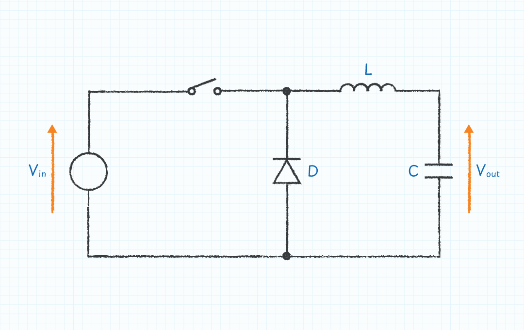
Figure 1 shows a buck converter design comprising a switch, inductor, capacitor and diode. To simplify equations and aid understanding of the operation we will assume an ideal switch and diode with Vsw = 0 and Vd = 0 throughout the following analysis. In a full detailed design to accurately determine the required Inductance value L, expected duty cycle D and operating efficiency, Vsw and Vd will be non-zero and it is important to include their effects.
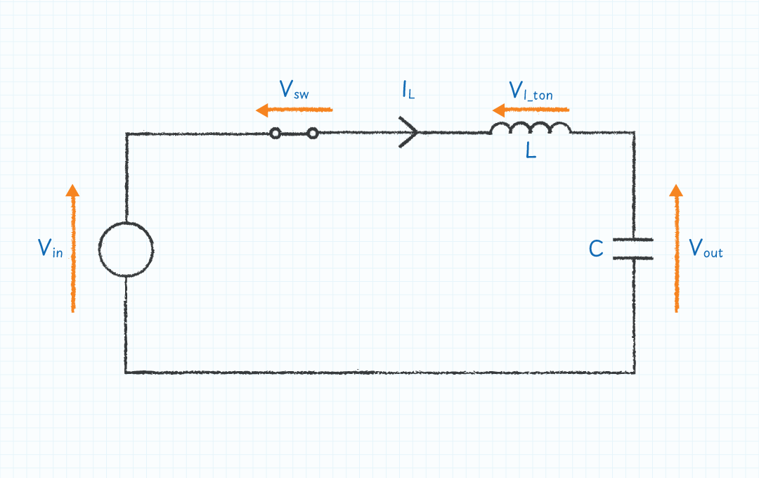
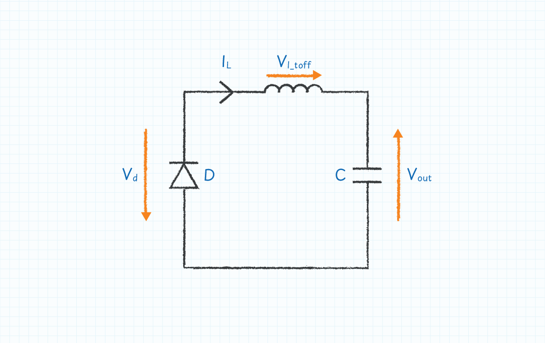
During the switch ON time the diode is off and the circuit reduces to Figure 2a with a ramping current flowing directly from the input to the output. During the switch OFF time the voltage across the inductor reverses in polarity as the inductor tries to maintain the previously flowing current, turning on the “catch” diode as shown in Figure 2b. The current now ramps down until the switch turns on again and the cycle repeats. The ramping ON current increases the inductor core magnetization, storing energy into the inductor, which is returned during the OFF cycle as the current ramps down.
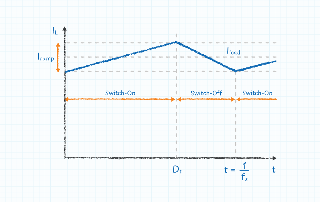
Figure 3a shows the inductor current waveform for the buck converter, which can be seen to include an average DC component and the ramping up and down AC component. The average DC current in the inductor is equal to the DC load current and under steady state conditions the total inductor current at the end of the cycle equals the value at the start of the cycle.
From the controlled switching action we have:

where D is the duty cycle and D = / ( + ).
Since the switching frequency = 1 / ( + ) we have = D/ .
Summing the voltage drops around the circuit during the switch ON time in Figure 2a with = 0 gives

Substituting = L * di/dt where di is the magnitude of the current ramp and dt is the ON time gives

Understanding Inductor Current Dynamics
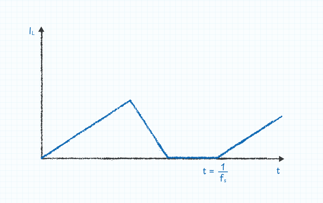
For a given input to output voltage difference, switching frequency and therefore , the right hand side of eq 3 is constant. Choosing a large value of inductance L gives a smaller ramping current component, while a smaller value of inductance gives a larger current ramp. If the inductance L is made very small the current ramp may become so large that under low load current conditions the total inductor current can become zero for part of the switching period. This is called discontinuous mode and is shown in Figure 3b as opposed to the continuous mode in Figure 3a where the inductor current never reaches zero
While a smaller value of inductor may be attractive in some applications, a larger inductor ramp current leads to higher output voltage ripple since this is determined by the inductor current ramp amplitude and the output capacitor's capacitance and Equivalent Series Resistance, or ESR. A very high value of also leads to increased inductor AC core losses and temperature rise as the inductor core is repeatedly magnetized and demagnetized. Generally is chosen to be small compared to the maximum load current and this choice determines L the inductance value.
Maximum Peak Inductor Current
A key specification is the maximum peak inductor current, calculated as:

From equation 3 we saw that is independent of . In order to determine we need to consider how varies for different Vin once the inductor L is fixed.
Summing the voltage drops around the circuit of Figure 2b with = 0 during the OFF time we have

Substituting = L * di/dt where di is the magnitude of the current ramp and dt is the OFF time gives

Since is constant, is a maximum when is at a maximum, which occurs when is at a maximum and this input condition is therefore used to determine and the maximum peak inductor current in equation 4.
Once the required inductance and maximum current are known a suitable inductor can be selected. It should be noted that the higher the inductance and maximum current, the larger the physical size of the inductor. Increasing the inductance requires more turns of wire on the inductor, thereby increasing the length of wire and winding volume. Increased length of wire increases the winding's DC resistance, another key inductor specification impacting on energy losses, heating and efficiency. Increasing the inductor current requires a larger wire diameter for low DC resistance, also increasing winding volume. Increasing the product of current and winding turns or “current turns” produces a larger magnetic field in the inductor core, increasing the core's magnetic flux density closer to its saturation limit. At saturation the inductor stops acting like an inductor, its inductance drops and higher current flows. The inductor's saturation current specification is typically the point at which the inductance has dropped by 10% or as much as 35% depending on the core construction type - see the inductor datasheet notes. To increase the saturation level to allow higher currents requires a larger core.
Trends in Switching Converter Design
A major trend in switching converter design is towards higher switching frequencies, which leads to a smaller total switching period with shorter and . This allows a lower inductance value L and/or a lower value of Iramp for a given input and output voltage (equation 3), and therefore a physically smaller inductor. A disadvantage of increasing the switching frequency is an increase in switch losses, which may impact efficiency negatively depending on the overall changes made.
Equation 4 only gives the maximum current during steady state operation. Another consideration is the control IC's internal current limit, as during start up or load transient conditions, higher peak currents may be seen than the steady state value calculated. It may be beneficial to incorporate extra design margin on the inductor's maximum allowed current to avoid any unwanted saturation effects at these times.
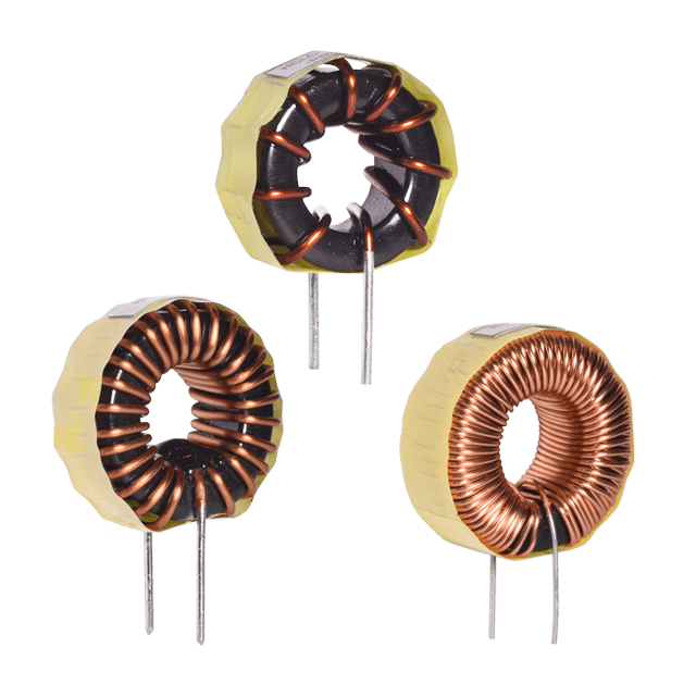
Choosing the Right Inductor
Signal Transformer offers 2,700 standard SMD inductor part numbers split across various series with:
- Inductance values ranging from 0.01uH to 10mH
- DC current capability ranging from 4mA to 70A
- DC resistance ranging from 2mΩ to 140Ω
- Height ranging from 1mm to 12.3mm
- Custom formulated powder materials
- High efficiency
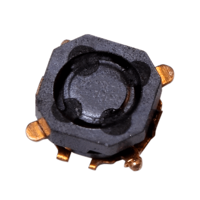
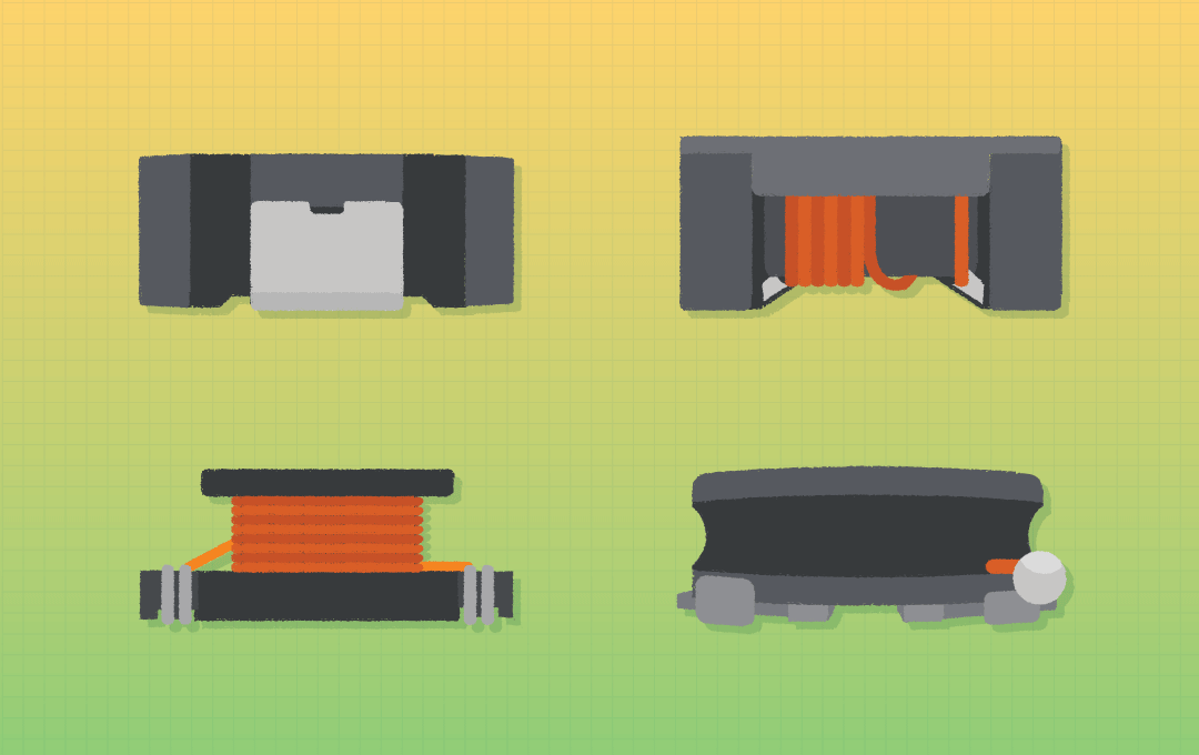
Different surface mount (SMD) inductor construction types are available to suit different needs including unshielded, shielded, low profile and low EMI families.
For compact densely populated board designs, as typical in new IOT designs, the shielded and low EMI inductors are good choices, since their magnetic flux is better contained within the inductor resulting in lower noise induced in surrounding PCB traces and components. The SCRH series of magnetically shielded parts are available with inductance values ranging from 1.0µH to 180µH, saturation currents from 0.15A to 5.0A and heights from 1.9mm to 4mm. If a larger inductor value is required the SCxxxxC series includes values from 10µH to 1mH, with saturation currents from 0.045A to 8A and heights from 2.92mm to 7.62mm.
For high current the SCEP series includes inductance values from 0.15µH to 27µH with heights from 4.5mm to 8.1mm and saturation currents from 4.5A to 70A. The SCIHP shielded high current series offers inductance values ranging from 0.22µH to 22µH suited to high frequency applications up to 5MHz with saturation currents from 2.0A to 48A and heights from 1.8mm to 6.7mm.
For highest efficiency and power handling, unshielded types can offer best performance and are available in low profile for when height is an issue. For lowest profile the SCMD4D series includes inductance values from 3.3µH to 100µH, with 1mm to 1.45mm height and 0.16A to 1.55A saturation current. The SC1206, SC1210, SC1812 and SC2220 series named after the popular standard PCB footprints cover together a range of inductance values from 0.1µH to 10mH, ranging in height from 2mm to 5mm with saturation currents from 0.05A to 7.8A.
Inductor Tolerance and Testing
As with any component, inductor values are specified with a tolerance that, for Signal Transformer inductors, is typically +/-10%, +/-20% or +/30% depending on the type and value. This should be factored into choosing the right inductor value to meet your needs. Once an inductor has been selected it is important to obtain samples, build and bench test the complete DC-DC power converter design over the full expected operating range including the full input voltage range, all load current conditions, start up conditions into any expected loads, and under all operating temperatures to ensure it operates as expected over all corner conditions.